Free Returns Guarantee
Free & Easy Returns
Free & Easy Returns

Thermal Imaging is an indispensable tool in electronics failure analysis, enabling engineers to quickly identify device issues. When electronic devices fail, time is critical, and traditional methods like multimeter probing, signal tracing, or X-ray inspection can be slow, invasive, or inconclusive. Thermal Imaging provides fast, non-contact visualization of heat patterns, often revealing the root cause of failures. This article outlines a typical failure analysis workflow, demonstrates how Thermal Imaging accelerates problem localization, and shares practical engineering cases where thermal inspection made troubleshooting faster and more accurate.
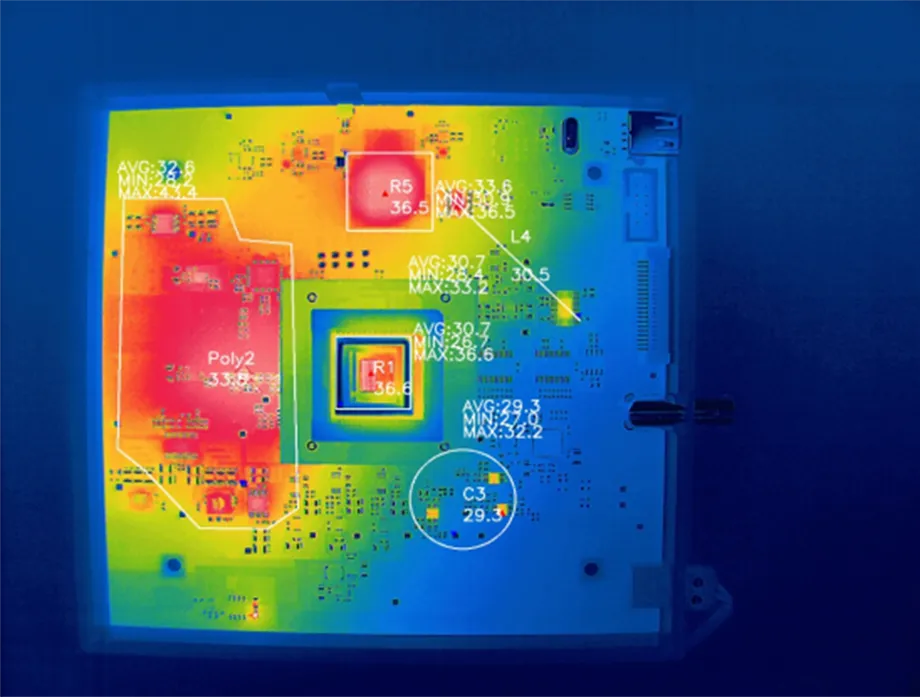
Here are striking thermal images of overheating PCBs during failure analysis, clearly showing hotspots that indicate the source of failure:
A standard failure analysis process for electronic devices typically follows these steps:
Thermal imaging shines in step 3, often reducing the time spent in later, more destructive phases by pinpointing the problem area quickly and accurately.
The HANMATEK TI240 thermal camera, with its 240×240 pixel resolution and high thermal sensitivity (detecting differences as small as 0.08°C), provides an immediate thermal "fingerprint" of the operating circuit. Abnormal heat patterns almost always indicate the fault location:
This non-contact approach allows engineers to scan the entire board in seconds while the device is powered and operating under fault conditions — something impossible with traditional point-contact methods. It guides subsequent probing, reduces guesswork, and minimizes risk of further damage during diagnosis.
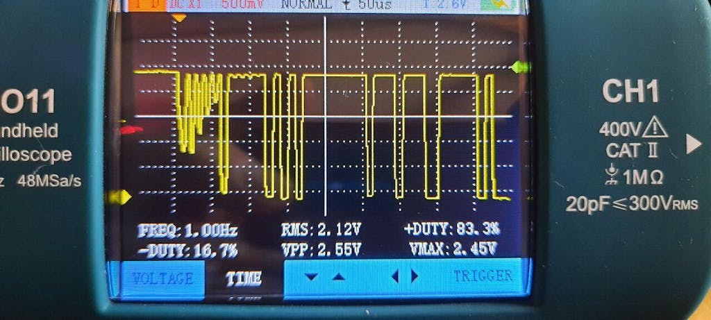
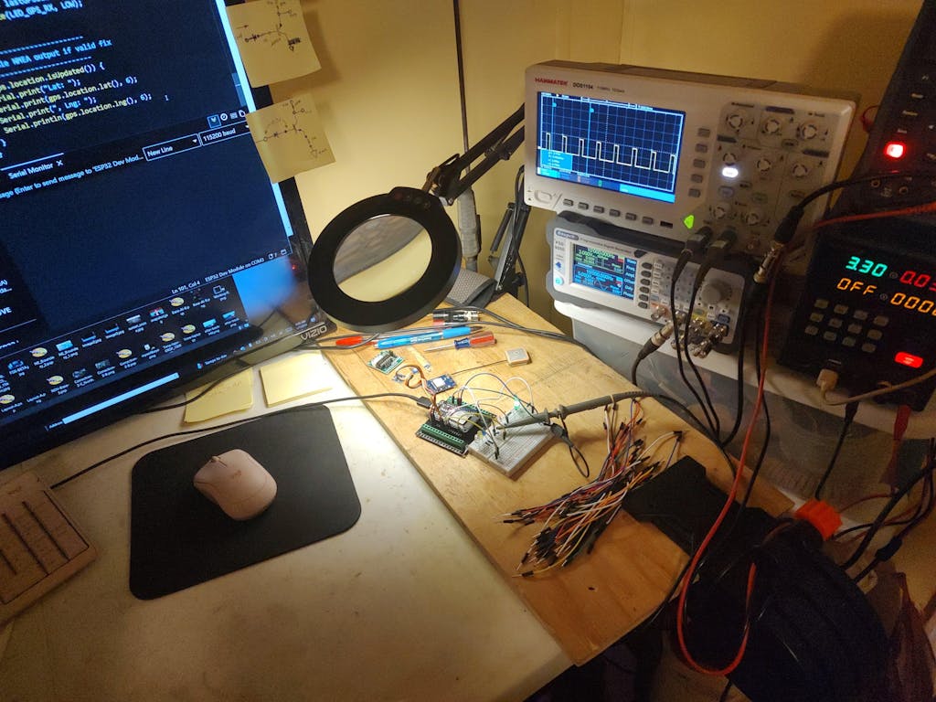
Watch a handheld thermal camera in action during real electronics fault detection and failure analysis:
Case 1: Intermittent Power Supply Failure A customer-return power adapter exhibited random shutdowns. Visual inspection showed no damage. Using the TI240, the engineer quickly identified a single MOSFET running 45°C hotter than its counterparts — revealing a marginal gate drive issue. Fixing the driver circuitry resolved the problem in under 30 minutes.
Case 2: Smartphone Motherboard No-Power Issue After water damage, the board would not power on. Thermal scan under low-voltage injection revealed a tiny hotspot on a power management IC. Closer inspection confirmed a micro-crack in a capacitor nearby. Replacing the affected components restored functionality.
Case 3: Industrial Controller Overheating An embedded controller in a factory machine was shutting down sporadically. The TI240 scan showed uneven temperature distribution across voltage regulators. Analysis revealed poor thermal vias under one regulator — a design flaw that was corrected with additional vias and heatsinking.
These examples demonstrate how the HANMATEK TI240 turns hours of blind troubleshooting into minutes of targeted investigation. For full product details and to add this powerful tool to your failure analysis toolkit, visit the HANMATEK TI240 product page.
In conclusion, incorporating thermal imaging into your electronics failure analysis process is no longer optional — it's a competitive advantage. The HANMATEK TI240 delivers professional-grade performance at an accessible price, empowering engineers to find, fix, and prevent failures faster than ever before. Upgrade your lab today — explore the HANMATEK TI240.
{"one"=>"Select 2 or 3 items to compare", "other"=>"{{ count }} of 3 items selected"}


Leave a comment